Physical Device
This describes the carriers (electron and hole) in the semiconductor material.
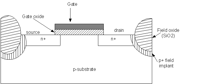
Figure1. Cross section of NMOS transistor
A cross section of a typical n-channel MOS transistor (NMOS) is shown in Figure 23.Heavily doped n-type source and drain regions are implanted (or diffused) into a lightly doped p-type substrate. A thin layer of silicon dioxide (SiO2) is grown over the region between the source and drain and is covered by a conductive material, most often polycrystalline silicon (or polysilicon, for short). The conductive materials form the gate of the transistor. Neighboring device are insulated from each other with the aid of a thick layer of SiO2 (called the field oxide) and a reverse-biased np-diode, formed by adding an extra p+ region, called the channel-stop implant(or field implant).[5]
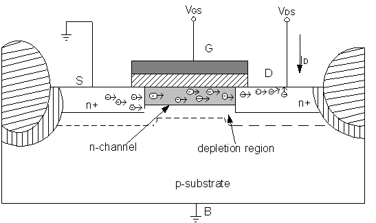
Figure2 NMOS transistor with bias voltage
To show the switching feature of MOS transistor, take NMOS for example. As shown in Figure 24,assume now that a positive voltage is applied to the gate (with respect to the source).The gate and substrate form the plates of a capacitor with the gate oxide as the dielectric. The positive gate voltage causes positive charge to accumulate on the gate electrode and negative charge on the substrate side. Hence, a depletion region is formed below the gate.
As the gate voltage increases, the potential at the surface at some point reaches a critical value, where the semiconductor surface inverts to n-type material that is known strong inversion phenomenon.
Further increases in the gate voltage result in additional electrons in the thin inversion layer directly under the oxide. These are drawn from the heavily doped n+ source region. Hence, a continue n-type channel is formed between the source and drain region.
1. Open source resources
PISCES: Advanced 1D and 2D Device Simulation for Silicon
2. Web pages
IBM publish its research on physical device:
http://www.research.ibm.com/people/l/lipscomb/www-joy.html
3. Citations
<<Compound Semiconductor >>magazine is a good reference of current development of semiconductor device.